




HASS Produces 200mm-Class Experimental Glass Substrate Samples
2026-10-08
120
“Achieves Flexural Strength of 440 MPa, Approximately Twice That of Conventional Borosilicate Glass”
By Kyung-yoon Jang
HASS, a glass-ceramics company, announced on October 6
that it has achieved significant progress in its semiconductor packaging glass substrate research under the Ministry of Trade, Industry and Energy's Materials and Components Technology Development Program.
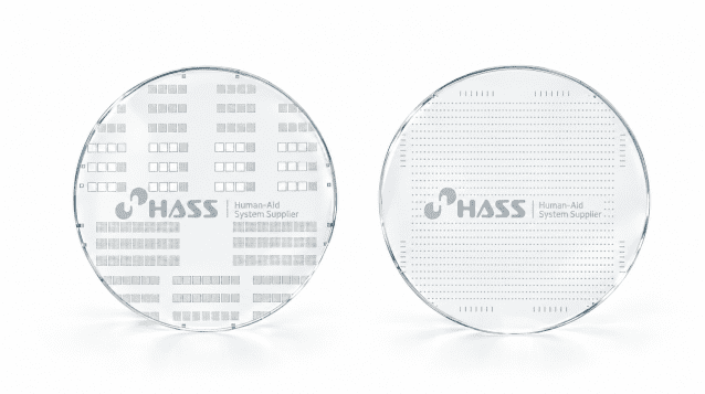
Key achievements include the successful fabrication of large-area glass substrate samples measuring approximately 200 mm in diameter and the development of high-strength glass materials.
HASS recently held a workshop and seminar with participating research institutes, universities,
and companies to present the progress of a government-funded research project launched in 2024.
The project, titled “Development of Wafer-Type Aluminosilicate Glass Substrates and Photochemical Reaction-Based Via Hole Processing Technology for Diameters of 10 Micrometers (μm) or Less,”
is led by HASS as the principal research organization.
The government-funded project runs for 54 months, from July 2024 through December 2028, with government funding totaling KRW 2.75 billion.
HASS and its research partners aim to develop 300mm-class wafer-type glass substrates,
through-glass vias (TGVs) with diameters of 10 μm or less, and low-dielectric, low-loss glass materials and processing technologies for semiconductor packaging applications.
As part of the collaborative research, HASS is responsible for designing UV-sensitive glass-ceramic compositions and developing large-area glass forming processes.
The company is leveraging approximately 20 years of expertise in controlling crystalline microstructures,
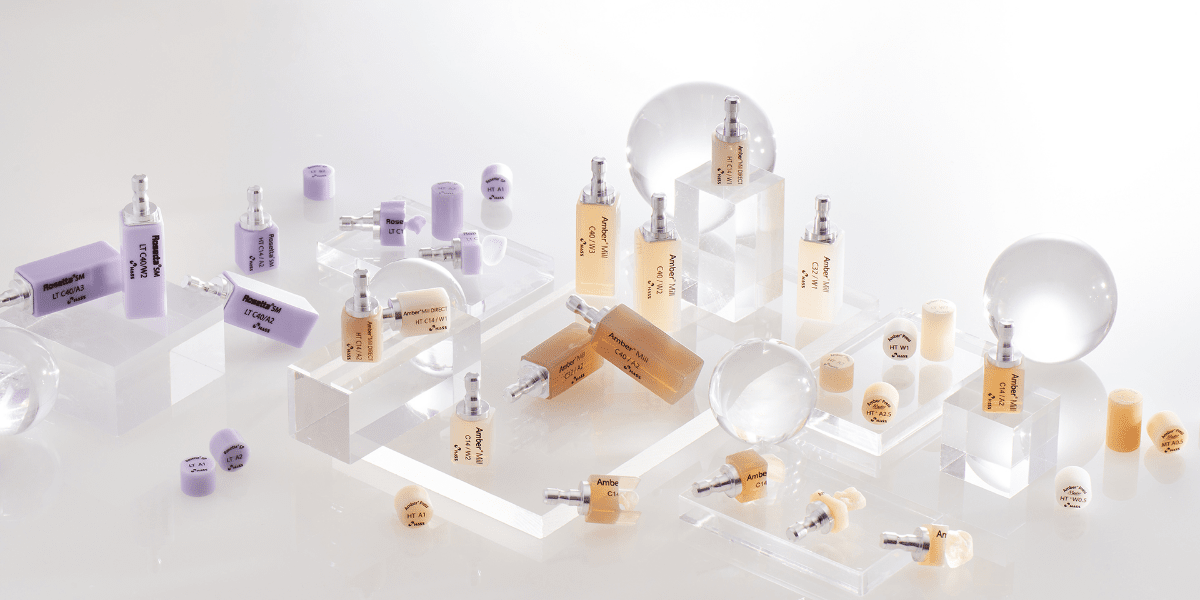
accumulated through its work in dental glass-ceramics, to expand its technological capabilities into semiconductor materials.
HASS stated, “Together with our research partners, we recently succeeded in fabricating large-area glass substrate samples measuring approximately 200 mm in diameter.
We also confirmed the feasibility of forming through-glass vias (TGVs) using 100mm-class glass substrates made from the same material.”
Under identical testing conditions, the newly developed material demonstrated a flexural strength of approximately 440 MPa, roughly twice that of conventional borosilicate glass.
The research team also successfully formed TGVs with uniform hole dimensions on both the front and back surfaces of glass substrate samples approximately 1.5 mm thick.
Building on these achievements, HASS continues to refine its glass composition design and large-area forming processes.
Glass substrates are attracting increasing attention as next-generation semiconductor packaging materials amid the rapid expansion of the artificial intelligence (AI) and high-performance computing (HPC) markets.
In principle, compared with conventional organic substrates, glass substrates offer superior surface flatness and lower thermal deformation, making them well-suited for fine-pitch interconnections and stable signal transmission.
SEMI, the global semiconductor industry association, has projected that initial production of glass-core substrates could begin around 2028.
Original Article